Using the LPSPI and eDMA Controllers for Digital Waveform Synthesis.
Aug. 21, 2024
Eli Hughes
Jerry Palacios
Introduction
The Serial Peripheral Interface (SPI) is ubiquitous in embedded systems for interfacing to external peripherals such flash memories, EEPROMs, analog to digital converters and sensors. SPI is a synchronous serial data transmission standard which has a data path from a controller to a peripheral and vice-versa. Data bits are sent synchronous to a clock and there is typically a “chip select” signal to flag an active transaction with a downstream peripheral.
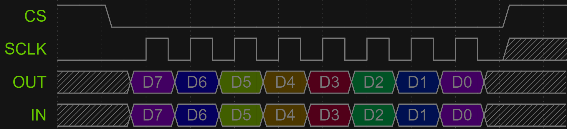
1-byte SPI Transfer in 0,0 Mode. Data Is sampled on the rising edge and shifted on falling edge
Most peripherals expect some sort of multi-byte transaction where data from the controller has an address and/or command structure. At the core of typical SPI controller is a shift register. The shift register is often surrounded by logic to control clock phase, the chip select signaling and input data loading.
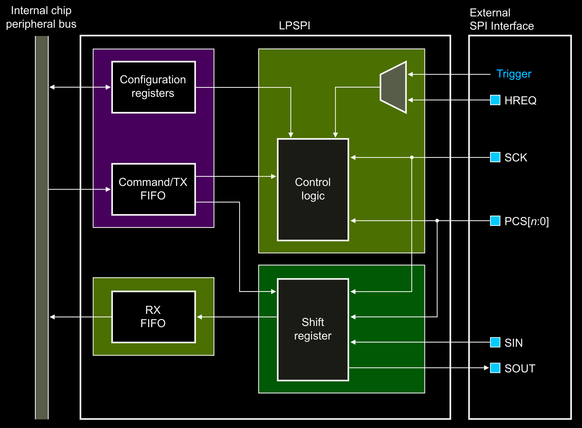
The LPSPI Peripheral in the NXP MCXA15x Family of Microcontrollers
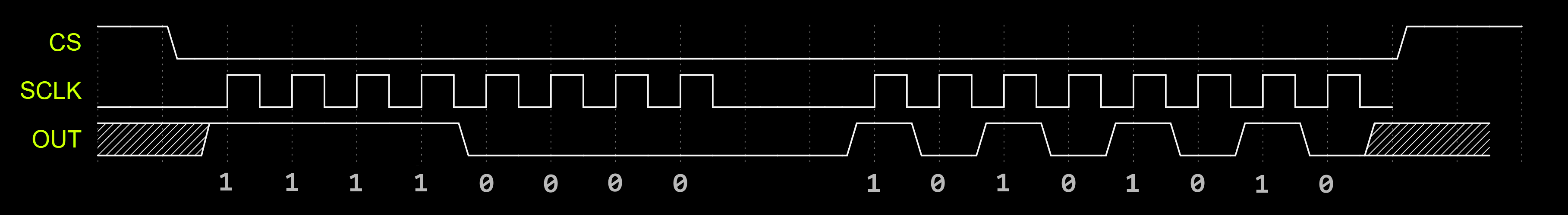
Once you understand that SPI is implemented with a shift register with control logic, you can envision using it for applications outside of the typical use cases. Consider the scenario where the bytes 0xFF and 0xAA are transmitted with a chip select.
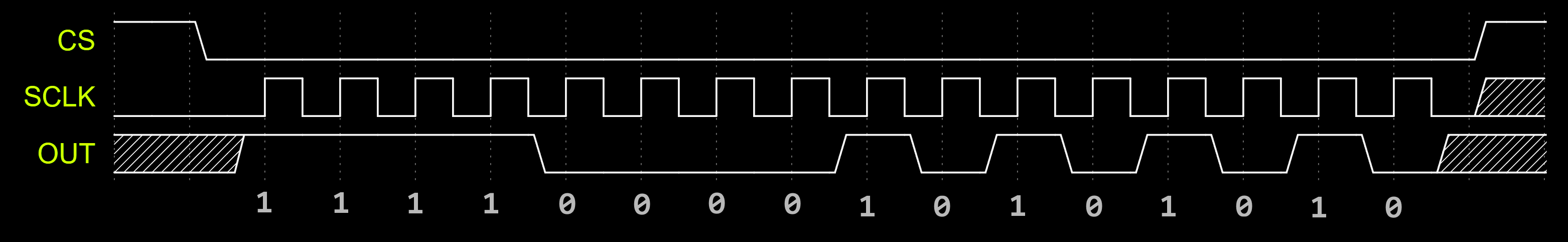
This example is shown with a gap between data bytes. This is not uncommon for simple MCU software SPI implementations that might poll for when data can be written to the shift register. The MCXA153 has FIFOs in front of the core shift register. This enables the MCU to keep the shift register loaded with data to generate a continuous stream.
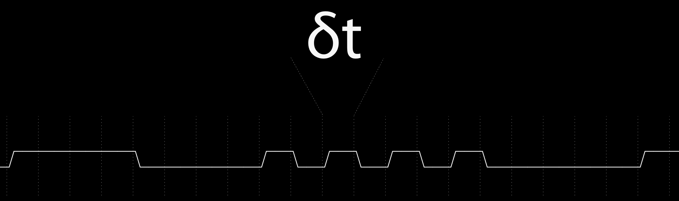
In this example, we assumed 8-bit transactions. The SPI controller in the MCXA153 can shift up to 32-bits at a time. Next, let’s remove the chip select and clock signal and then consider the data signal as long series of data bits.
Precise control of a data stream with a fixed time quanta
If the SPI output shift register is kept loaded with new data as the prior data is being shifted out, we can synthesis arbitrary data patterns with a precise time quanta. The SPI peripheral still has a clock, we are choosing not to expose it. The time quanta δt is set by the internal clocking to the SPI peripheral.
Synthesizing a continuous waveform pattern is achieved by using Direct Memory Access (DMA). The MCXA153 has a DMA controller which can automate transfers of large blocks of data to the SPI peripheral to ensure a 100% continuous data stream
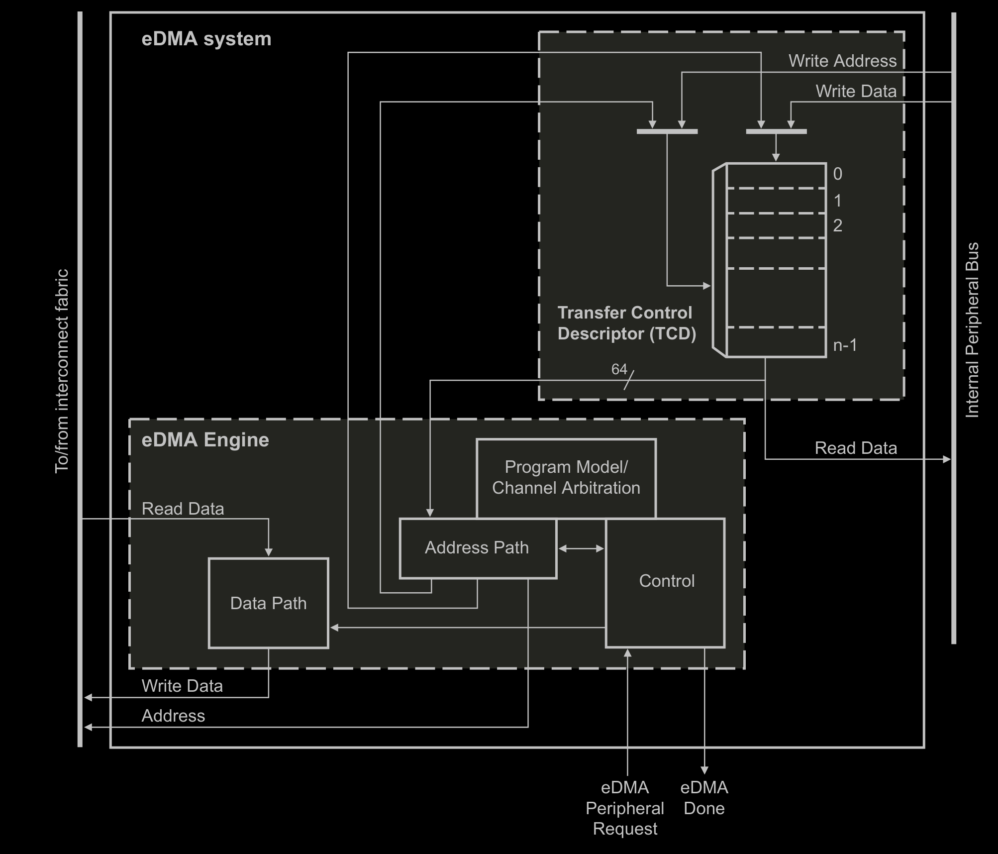
The MCXA Family eDMA Controller
The desired waveform is precomputed, then DMA is used to transfer large blocks of the precomputed data to the SPI peripheral for a continuous data stream. DMA transactions can be linked using a “ping-pong” buffer scheme. The MCU can pre-compute the next data buffer while the DMA controller is moving the current buffer.